
PCB Layout
Inroduction
PCB Layout/Routing is the next step after component placement in PCB design work. It is the actual physical point-to-point connection of nets driven by the circuit schematic. All of this design work from schematic capture to component placement until PCB routing are done through EDA CAD software tools (Cadence Allegro in our case).
PCB layout topic is a very broad field and involves many steps and guidelines to complete the design process. Discussions here will be limited to aspects relating to embedded design systems. PCB layout work, in general, is not just connecting traces but also includes making a specification of the PCB that meets the requirements of the project. This involves determining what PCB technology to use (double-sided or multilayers, through-hole vias or blind/buried/laser vias, trace width/spacing, layer stack-up, etc). It all depends on the complexity of the circuit and its required features. After making a PCB specification, connectivity work can begin until all nets are connected. The final output of this is generating, what are called in the PCB industry as Gerber Files and fabrication drawings, which are then being sent to a PCB fabricator to build the PCB.
In summary, PCB layout is the final electrically-related design work of putting the whole project concept into its physical reality. Though this is schematic-driven from circuit design, it can also “make or break” a project if its not done properly.
Snapper


PCB layout stages:
Determining the electrical requirements
Embedded systems can have the same features as a normal desktop PC have, depending on its target application. Though it may be slower in speed compared to most modern PCs, it still employs the same basic circuit requirements (CPUs, SDRAMs, Memory storage, etc.) and interfacing options (LCDs, USB, Ethernet, Wi-Fi, Bluetooth, GPS/GPRS, Power-over-Ethernet, power supplies, etc.). Most of these have circuits that are critical in nature and employ high-speed electrical signalling (CPU to SDRAM interface, high-speed clock lines, differential signalling for USB/Ethernet and LVDS for certain types of LCDs, RF antenna traces, analog/audio signals, etc.) which require high-speed and mixed RF/Analog-Digital PCB layout techniques to be employed during routing and specifying PCB requirements (see PCB Design Guidelines). This usually requires controlled-impedances (single-ended/differential impedance) on traces carrying these signals and matching length these traces during layout. This will also determine the number of layers and layer-stack configuration build-up of the PCB. This will form the bulk of the PCB specification along with the required mechanical dimensions, PCB material and finish, silkscreen, soldermask and drill tolerance.
Determining the nature of electronic components used (fine-pitch surface mounts or through-hole)
Because of the requirement of the final product of most embedded systems to be small in size, small fine-pitch surface-mount components (BGAs, QFNs, DFNs, FCSP, etc.) are generally used. Development boards don't have this same restriction as the final product, so they may end up using standard component packages (SOICs, QFPs, through-hole connectors, etc). Knowing these components is another requirement that will determine the trace width/spacing and through-hole or blind/buried vias to use in the PCB. As the board gets very dense and highly complicated, so does the cost of building the PCBs and this will increase the cost.
Verifying the PCB specifications with a PCB manufacturer
When working with new PCB manufacturer or when special PCB requirements are needed (such as special PCB material for RF Gigahertz speed application), it is always best to check with the intended PCB manufacturer whether the PCB can be manufactured or if tweakings are needed at their end to meet the desired specification. This step is not necessarily needed if the designer is using a specific PCB vendor for quite some time and is already familiar with their capabilities.
PCB layout or routing
Having the prerequisites (electrical requirements and PCB specifications) determined in the first two steps above, the actual connection of nets or layout can commence keeping in mind all the critical circuits or areas that needed special care and applying good engineering practices when dealing with high-speed digital, RF/analog or a mixed of both. It generally make sense to route these difficult areas first and by-hand rather than relying on an Autorouter. In small embedded systems where you have limited space or room, doing the layout by-hand is almost always the best approach. Autorouter usually comes into play when routing non-critical areas of the board and when working with large development boards where space or room is not an issue. Another important thing to consider is Design for Manufacturability (DFM see Design for Manufacturability for details) to ensure that the overall PCB, from component placement to layout, is manufacturable.
PCB layout review
This is always done in concurrence with the circuit design engineer and sometimes, people from manufacturing and assembly for large volume production. For very critical boards, it is always best to do a review after the critical areas are done and another review when the whole layout is completed.

- Gerber generation/netlist verification, fabrication drawing
Gerbers are standard output files from PCB CAD software (Cadence Allegro) sent to a PCB fabricator and used to build the PCBs. Before these are sent, it is always advisable to do some visual checkings on these files as these are the link between the design files and actual PCB. Another method of checking is IPC356 netlist verification. It extracts a netlist out of the gerber files, compares this netlist from an IPC356 netlist format generated by the PCB CAD tool and generates error reports if it finds any discrepancies. This is a more sure way of verifying that gerber files and PCB design files are in sync.
Panelisation

This involves putting all individual PCBs in one PCB outline (panel) to make the PCB production and assembly efficient. This is mostly beneficial to mature products with large volume productions. Panelisation requires familiarity with PCB assembly house's capability such that the creation of the panel complies with their requirements and is optimised to get the most benefit. But most PCB assembly houses have the same basic requirements except in some situations where the product itself requires complicated PCB fab and assembly.
Bluewater Systems Experience


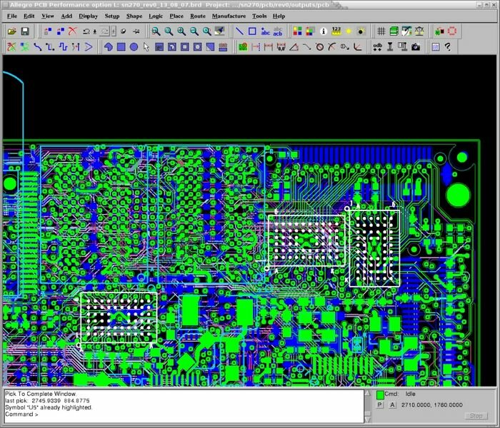
Bluewater Systems has designed a wide range of embedded system PCBs from very small form-factor and highly dense (e.g. Snapper System Modules) to fairly reasonable size development boards which are fairly densed and highly populated PCBs such as Rig 200 and DDS XM-100 storage series. The Snapper module PCBs, despite its very small form-factor of just 40x70mm, are packed with wide range of features and using very fine-pitch SMT components (BGAs, QFNs, etc.), was designed to be built just using conventional PCB fabrication methods, thus keeping cost in check. The PCB is 10-12 layers, impedance-controlled, 8mil drill through-hole vias and 4mil trace width/spacing. The PCB layout could have been easier if it was designed to be build using High Density Interconnect (HDI see which usually involves highly sophisticated microvia, blind/buried microvia laser drilled and requires unique fabrication methods, but this would drive the cost higher.
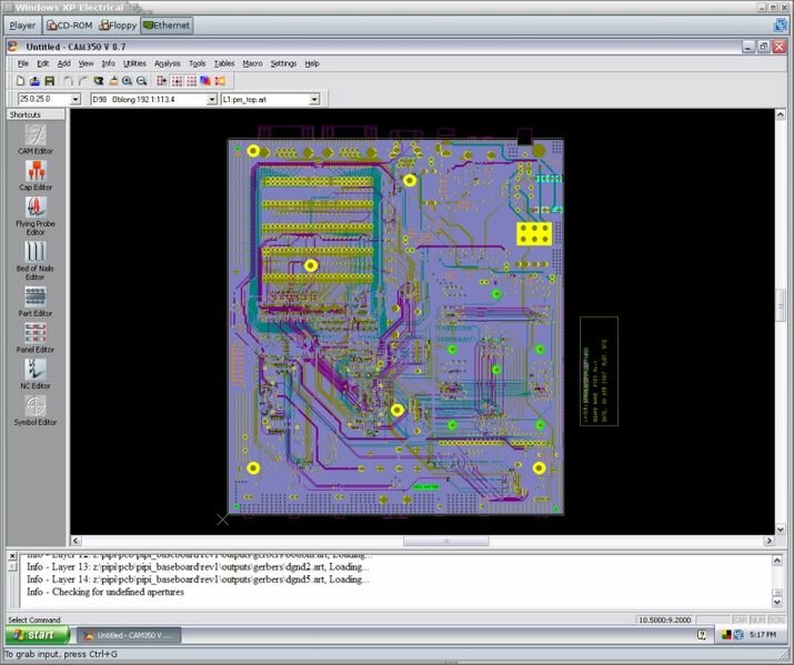
In one particular Snapper module, called Snapper270, two 56-ball BGA at 0.65mm pitch were used because of their small size. This is a very fine-pitch BGA. To fan-out the pads, it would normally require laser-drilled blind/buried microvia. But through careful component placement, pinout assignments and routing strategy, we were able to get away with it and just use conventional through-hole vias during fan-out and kept the cost low (see snapshot of this below with the fine-pitch BGAs highlighted.
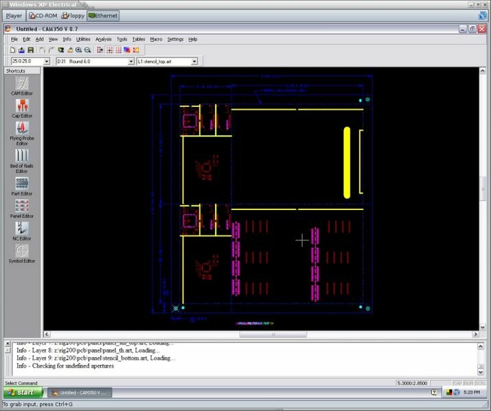
Rig 200 PCB Layout
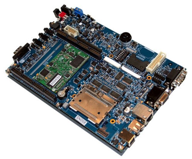
The Rig 200 PCB, with its form-factor derived from a standard 5.25 inch CD-ROM bay, measures 199mm by 140mm. But packed will all the features one can think of, ended up being a highly-densed populated board and so does the routing with the addition of a Snapper SO-DIMM version support.


