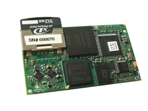
During development of our new Snapper 9260 module, one of the requirements was for boot times (power -> prompt) of less than 6s. Since the (rather feature-rich) development system boot time was in the order of 45s, there was quite a bit of scope for improvement: - Enable MMU and data cache in U-Boot: by default, U-Boot does fairly minimal initialisation of hardware. We extended main board support and network driver code to support making full use of the instruction cache (easy) and data cache (a bit more interesting). Time saving: ~3s. - Use on-board storage for kernel and root filesystem, instead of NFS. Time saving: ~2s. - Rationalise U-Boot environment: remove the boot delay, flatten out dynamically-generated bootup scripts, use uncompressed image (or gzip-compressed image if space is a constraint) instead of self-decompressing image, disable redundant image verification. Time saving: ~2s. - Strip unneeded drivers out of Linux kernel: by removing unneeded systems (eg. networking, unneeded filesystems, debugging facilities, splash logo), we reduced the Linux kernel size from 3.6Mb to 1.8Mb. Time saving: ~1.5s, plus reduced kernel boot times. - Add 'quiet' to Linux boot arguments, suppressing synchronous printk output. Unlike removing printk support entirely, the bootup messages are still available via dmesg, supporting field debugging. Time saving: ~2s. - Preset loops-per-jiffy setting for Linux kernel. Time saving: ~0.25s. - Strip filesystem to avoid unneeded subsystems, slow init() scripts, minimise footprint. Time saving: ~30s. Overall, these changes allowed us to reduce the boot times for the unit to 5.2s - well within the 6s target - without sacrificing support for interactive access and field upgrades. We hope to gain another 1.2s back between power-on and start of execution by using a new revision of the AT91SAM9260 chip (an erratum on the 'A' revision silicon), which should bring overall time below 5s - not bad for a full-featured Linux device!

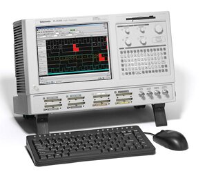
Earliest Snapper coming to the end of its lifePosted in Uncategorized on January 15, 2009 by Daniel Keis In 2004 the first Snapper Single Board Computer Module was designed by Bluewater Systems. Snapper 255 is a powerful module which incorporates an FPGA, Ethernet, USB OTG, LCD with touchscreen, 64MB SDRAM and 512MB NAND Flash, all on a board smaller than a business card. Snapper 255 has been used in various designs since then but sadly is now coming closer to the end of its life. The Intel PXA255 microcontroller (now under the ownership of Marvell) that was originally used is unfortunately nearing the last time buy stage with no pin compatible replacement available. Marvell will sell stock as long as it is available, but the last time buy will be in the next six months. Grey market stock will still be available after this date but will prove to be more expensive. Bluewater will continue to sell Snapper 255s and liaise with existing customers to forecast future usage and ensure that sufficient stock is available. Snapper 255 is a great building block for embedded designs, proving to be a great tool to test product software before the final product is made. In saying this we have numerous other Snapper modules to take its place. AA battery powerPosted in Hardware design on January 05, 2009 by Russell Hocken Many devices are battery powered, and there is a wide range of battery technologies to choose from: Nicad, NiMH, Lithium, Alkali, etc. They all behave differently and have different caviets. We have designed many products to run off battery power. Often the battery is fixed for the product, however sometimes it is desirable to use a standard battery - such as an AA for example. The problem is there is no guaranteeing which AA a user will use. Nominally an AA battery is 1.5v and the current capacity can vary from 600mAh to 3000mAh. Furthermore rechargeable AA batteries are often 1.2v. A fresh Alkali AA battery can read as high as 1.7v. 3.3v is a common voltage for digital electronics, and it is quite tempting to connect up two AA batteries in series to produce 3.0v and assume that is the power supply sorted. Unfortunately, given the range of AA 'voltages' indicated above, and combined with the fact that battery voltage decreases based on load and capacity, this approach is not acceptable. What needs to be done instead in such a system is to have a boost converter to generate the system 3.3v. On a recent design we used a Linear Tech LTC3539. This works over an input range of 700mV to 5v and can provide up to 2A. If the input is above the system rail - as can happen with some fresh AA cells, the converter still regulates the output voltage (albeit not as efficiently). If the system rail is 3.3v, then the batteries will quickly fall beneath this threshold, so the power loss due to this is not great. If such a chip is used to generate a lower voltage rail, then system operating life will suffer more. Using such a chip to generate a 3v3 rail provides maximum battery life for the system and ensures the majority of energy is drawn from any AA cell before the batteries are 'flat'. How will TI's OMAP3530 change things?Posted in Industry News on January 05, 2009 by Administrator We have just completed a design based around Texas Instrument's OMAP3530 microcontroller. This is a high-end chip with lots of CPU performance (2000 Dhrystone MIPS) and a built-in 6-core DSP. We have tied it together with 4GB of flash and 256MB of DDR memory and lots of graphics output features to make something which we think will have great application in the digital signage market. So far we have the platform playing MPEG4 video with an alpha-blended overlay. It looks very slick for such a tiny wee board, and we are not even beginning to use the full features of the platform. As the Open Source support for this chip grows, it is going to be interesting to see what develops. The key difference between an OMAP3530 and a desktop PC CPU like the Pentium 4 is the level of integration. The OMAP chip includes a DSP capable of H.264 4CIF resolution full duplex real-time encode and decode, something your average modern PC struggles with. Without the DSP, the OMAP would struggle too. The OMAP chip includes video scaling and rotation hardware, something delegated to the graphics controller in a PC. The OMAP chip includes a NAND flash controller for storage, rather than the SATA used in a PC - but my laptop has a solid state drive which actually includes NAND flash, so the SATA is really just getting in the way. The OMAP chip also has a built-in USB controller, 3D graphics acceleration, SD card controllers and a direct CMOS sensor interface. The PC's processor (Pentium or whatever) uses separate chips, boards or even products for each for these. So the interest question is how long will it take for the PC to head down the integration route? The OMAP CPU is fast enough (or nearly) for most modern PC requirements such as web, email and office documents. For a limited portable screen resolution of 1024x768 or so it puts across a good effort. It seems to me that at least the bottom of the PC market may one day be served by devices such as the OMAP3530 and its successors. As if on cue, Ubuntu and ARM annouced recently that they are working on an Ubuntu release for higher end ARM platforms. “The release of a full Ubuntu desktop distribution supporting latest ARM technology will enable rapid growth, with internet everywhere, connected ultra portable devices,” said Ian Drew, vice president of Marketing, ARM. “The always-on experience available with mobile devices is rapidly expanding to new device categories such as netbooks, laptops and other internet connected products. Working with Canonical will pave the way for the development of new features and innovations to all connected platforms.”The focus is of course portable devices. But I wonder whether in 5 years time we will be using anything else? Protocol Analysis using a Logic AnalyserPosted in Uncategorized on December 15, 2008 by Andre Renaud For several of our projects we have had to use a Logic Analyser to determine the proper working of an existing system. The results of a captured session on the Logic Analyser is a large binary file representing the state of all 136 of its inputs, over a period of time, at around 2ns granularity. This gives an enormous amount of data which must be then viewed by the operator to determine where a problem lies. Some aspects of this can be eased through the user interface on the Logic Analyser - colouring relevant lines, or giving textual labels to certain values. But mostly it is a manual process. We have developed a protocol definition system which allows us to describe the protocol, and then automatically process the traces from the Logic Analyser, decoding the results into a human readable form. This give a double benefit - we can analyse an existing system to determine how it is working, producing our parser as we go, and once this is completed we can then run it against our own implementation to verify that it conforms to the original system. As the Logic Analyser is a completely generic digital interface, it can process almost any signaling system. Using this technique we have written protocol definitions for the following buses:
|
